The IEEE International Conference on Micro Electro Mechanical Systems (IEEE MEMS) is a leading global platform for showcasing microfabrication, MEMS design, and nanotechnology advancements. The IEEE MEMS 2025, held in Kaohsiung, Taiwan, continued this tradition by bringing together researchers, engineers, and academics worldwide. With 729 abstracts submitted and 328 accepted (an acceptance rate of 45%), the conference featured 72 oral presentations and 256 poster presentations, including open posters. This event provided valuable opportunities for knowledge exchange, networking, and collaboration, reinforcing its reputation as a premier event in the MEMS research community.
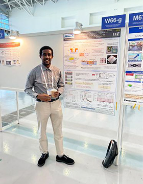
At the conference, I presented a poster titled "Enhanced Sensitivity of PtSi/p-Si Mid-IR Photodetectors through Narrow Electrode Spacing and Plasmonic Nanohole Structures." My research focused on developing a highly sensitive, uncooled mid-infrared photodetector using a 2D nanohole-array Au/PtSi/p-Si structure. The study explored the effects of reducing the electrode spacing from 4 mm to 2 mm, effectively suppressing carrier recombination and significantly enhancing the device's photosensitivity. The optimization resulted in a four-fold increase in specific detectivity (D*), demonstrating the effectiveness of narrowing the carrier path. During discussions, many attendees showed interest in the device’s potential applications in real-time chemical sensing and monitoring at room temperature. Questions also addressed the potential of applying this approach to other materials and whether additional design optimizations could achieve further sensitivity improvements. I explained that future research could involve exploring different electrode geometries and integrating advanced noise reduction techniques. These discussions provided valuable insights that will inform the direction of my ongoing research.
At this year’s IEEE MEMS 2025 Conference, my presentation, "Enhanced Sensitivity of PtSi/p-Si Mid-IR Photodetectors through Narrow Electrode Spacing and Plasmonic Nanohole Structures," received significant attention from the international research community. The poster session was an excellent platform to communicate my research's novelty and technical significance. I received enthusiastic feedback from numerous researchers interested in applying similar methodologies to their materials and exploring potential collaborations for future studies.
The conference brought together world-renowned experts in MEMS and nanotechnology, providing a valuable opportunity to discuss cutting-edge advancements in the field. I had particularly insightful exchanges with researchers from North America, focusing on plasmon-enhanced sensitivity enhancement of sensors and their novel applications. These discussions provided fresh perspectives on optimizing device performance and integrating new materials for broader sensing capabilities.
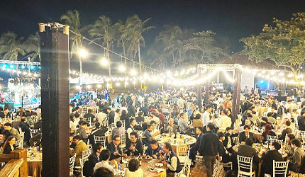
The five-day conference experience was enriching. It allowed me to present my research findings to a global audience and establish meaningful professional connections. This year's conference was unique and featured two banquet programs that provided an excellent informal networking platform and fostered meaningful connections with researchers from diverse backgrounds. These events facilitated engaging discussions beyond the technical sessions, encouraging the exchange of ideas and potential collaborations. The relaxed atmosphere of the banquets allowed for deeper conversations strengthened professional relationships and opened doors for future joint research opportunities. The diverse technical discussions and networking opportunities will significantly contribute to advancing my future research.
Finally, I would like to express my sincere gratitude to the Marubun Foundation for their generous support, which enabled me to participate and present at this prestigious international conference.
